


Process Technologies
Solution Examples
Single-Head, High-Speed Process
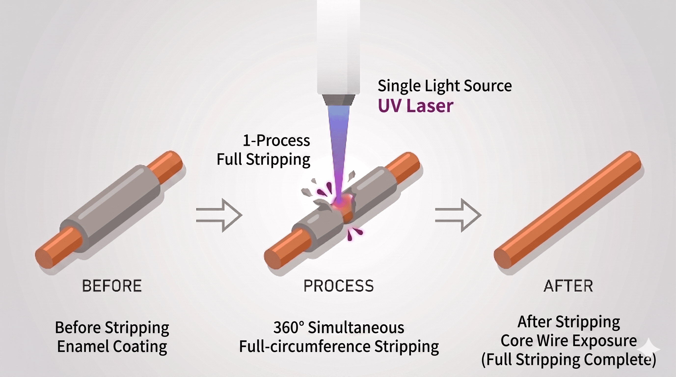
To protect the copper conductor, conventional processes required multiple scans using two different wavelengths, resulting in high capital costs and long cycle times.
Through optical design and process optimization, we achieved full-surface removal with a single light source and head, while suppressing damage to the copper. This reduces both capital investment and takt time.
No Additives — Clear Bonding
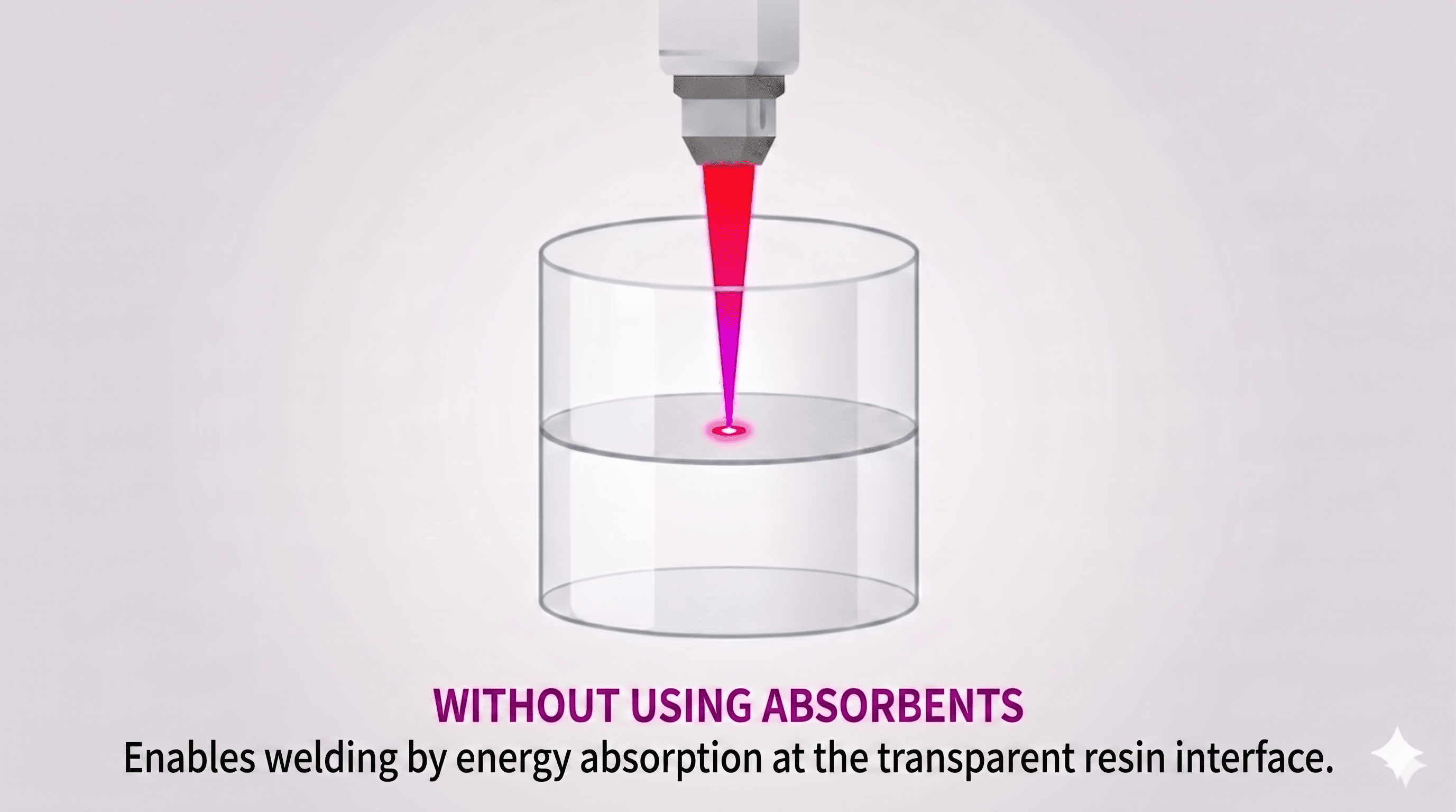
Joining transparent resins has traditionally required absorbers or adhesives — introducing contamination risk, compromised aesthetics, and the overhead of managing an additional application step.
Using our interface energy absorption control technology, we achieve direct welding of the base materials themselves — eliminating consumables and ancillary equipment for a clean bonding line.
Cost Reduction with Nanosecond Laser
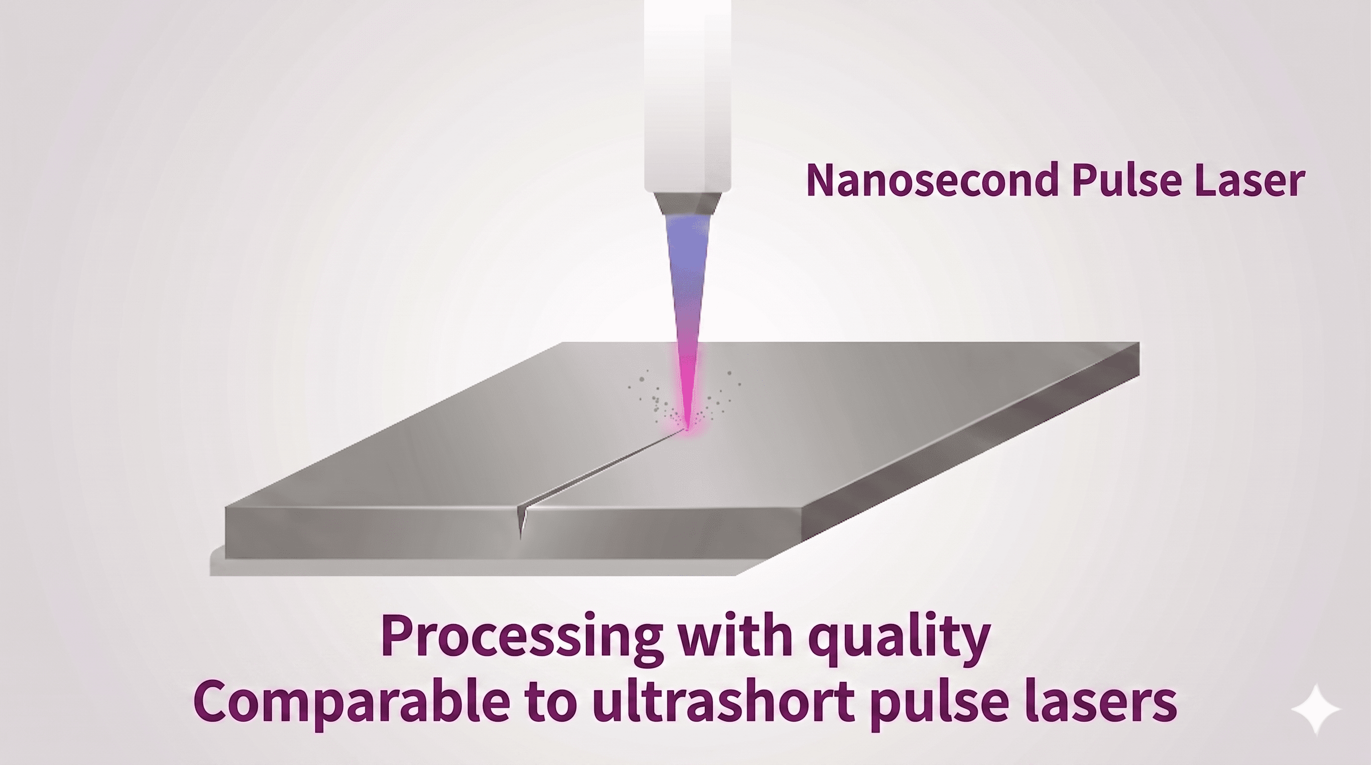
Cutting hard-to-machine materials was assumed to require expensive ultrashort-pulse lasers, whose depreciation costs drove up mass-production unit prices.
Through pulse control optimization, we achieved high-quality processing with a nanosecond laser — providing an alternative process that reduces the initial cost of mass-production equipment.
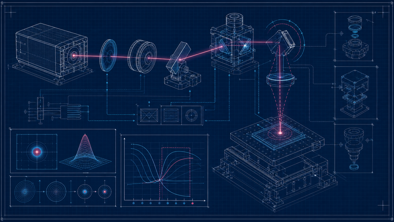
Core Technologies
Quantec's process technologies are not limited to the three examples above. Our core capability is to control the interaction between light, material, and production requirements.

Why Can We Do Them?
These solutions were not achieved by chance.
What wavelength, pulse width, and energy density should be applied to a given material to trigger the desired physical reaction? This “process design” is our core technology.

System Integration

Process Driven Design